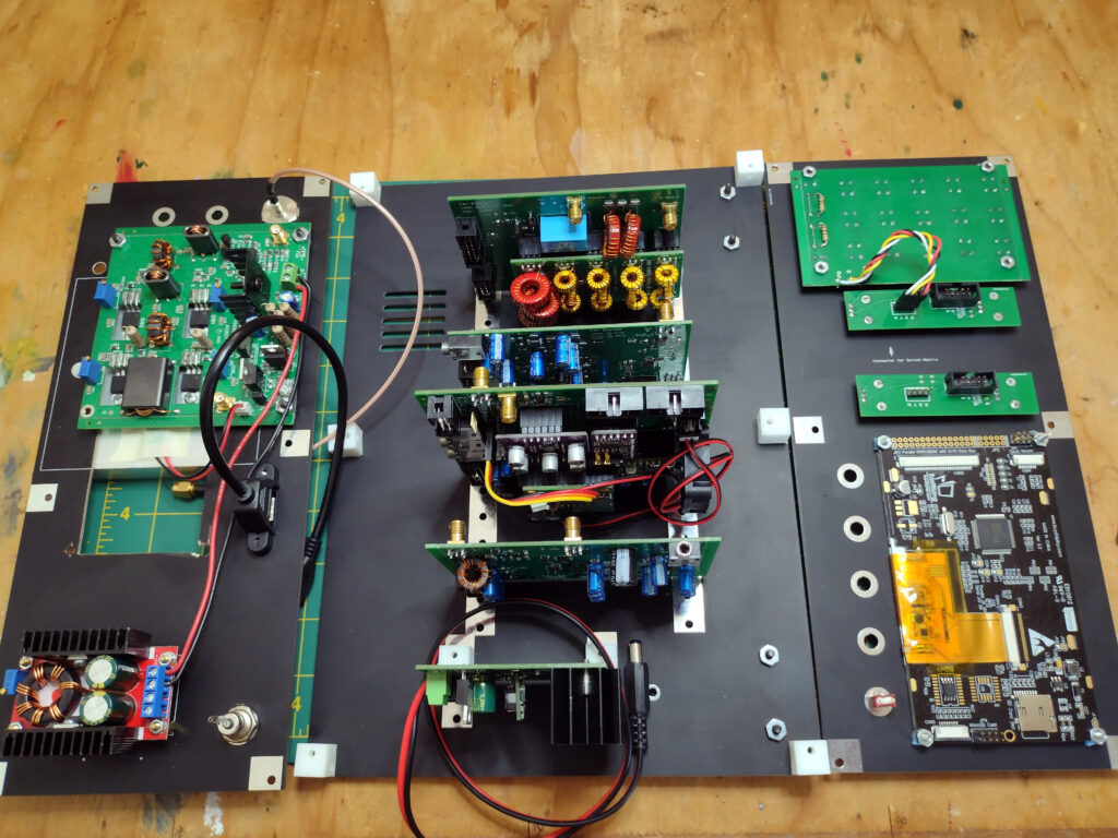
Construction is well on its way. All the boards are built and the transmitter has passed an important milestone. First a look at the assembly which currently consists of three panels.
On the left is the back panel which currently is home for the 20 watt Power Amplifier board and its boost supply. The middle is the base panel which is home for 5 boards, itemized shortly. The panel on the right is the front panel which accommodates the display, four encoders and an array of pushbutton switches.

Back panel
The 20W power amplifier board is the V10 original. It is claimed to be able to produce 20 watts power output across the various bands, using 4 each IRF510 transistors. For this, it also needs voltage higher than the 12 vDC used throughout the rest of the rig. That smaller board is a buck convertor that bucks 12 vDC up to 25 vDC.
Since ordering this kit, I’ve learned that the transistors used in this amplifier have a very steep frequency efficiency falloff that reduces power in the 10M band to something notably less than 5 watts. I don’t care for 20 watts across all bands, but really do want at least 5. So…. there’s another power amplifier waiting in the wings, and it is the reason for that extra open space in the back panel. It will be the subject of another post where Bob learns to handle small SMD components.
Base panel
The 5 boards attached to the base are, from the bottom of the picture to the top:
- the 12 vDC power supply
- the QSD, Quadrature Sampling Detector, board where RF signals are prepared for digital signal processing.
- the Main board which holds digital signal filters, the little Tiny 41 microcontroller which handles all the signal processing, system configuration details, and menu system. This board also houses interfaces for the display, encoders and pushbutton grid, along with some audio processing
- the Exciter board produces phase shift and SSB, Single Side Band, modulation
- lastly a filter board includes all the pesky toroids (aka torroids, or toeroids) for RF Low Pass and Band Pass filtering
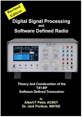
All of these functions are concisely explained in Al and Jack’s book: Software Defined Radio Transceiver: Theory and Construction of the T41-ep Amateur Radio SDT. About 500 pages which include a deep drive in Digital Signal Processing.
Note: there is now a 3rd version, which adds information for V12, version 12, of this radio.

Front panel
Self explanatory, a display board, 4 encoders, 16 pushbuttons and various other connectors.
Milestone – PA biasing
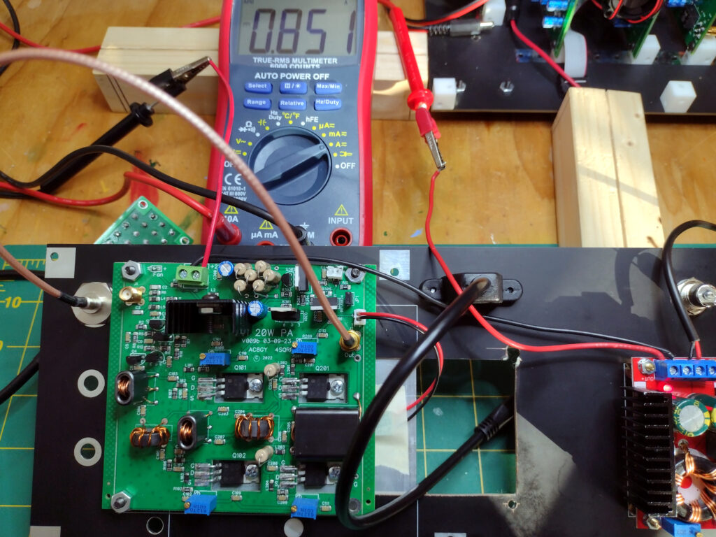
Even though I intend to replace the V10 Power Amplifier with another, I decided to complete the initialization, or biasing, of this amplifier. Maybe it can be used elsewhere sometime. The process is simple, and avoids smoke and explosions if each of the 4 blue potentiometers are first set to their lowest values (many turns counter-clockwise).
Then, an ammeter is placed inline with a 12 vDC power source and power is applied. The desired result is a base line of 50-55 mA for the board. One by one the blue potentiometers are turned up (clockwise) until the power drawn increases 200 mA for each IRF510 transistor. The end result is a current draw of about 850 mA and no smoke. Success. Done.
BTW, the finned aluminum heatsink, with no fan, reaches about 140 degrees F.

Next …
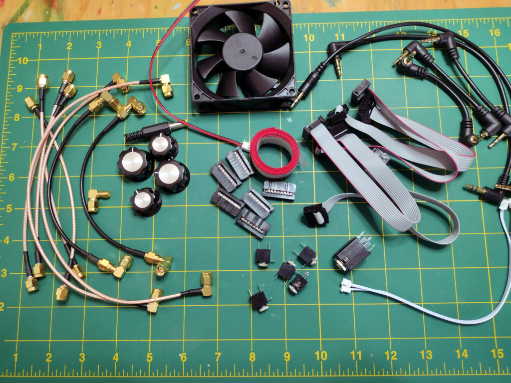
A whole bunch of interconnects, software loading, and various adjustment / alignment processes.

Leave a Reply